

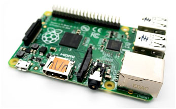
Did you ever notice that World is changing in 2X speed than it should have, there was a time when we used bulky phone’s, giant TV’s and huge radio’s. Time changed and improved technology made every gadgetstronger, smarter and smaller. Tiny transistors built integrated circuits and these circuits in PCB built all huge devices to be compatible, powerful.

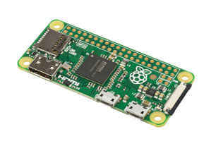
The world of engineers accepted PCB in building every technology and now it is considered as heart and soul of every smart device. It is in a remote to the latest rockets.PCB design has been around for decades, but its relevance is back in the spotlight. They originally came about to answer the need for smaller, more efficient ways to power electronics. In the age of The Internet of Things where everyday devices with embedded systems are becoming Internet-connected devices, PCB design is still meeting that need, while growing more advanced, and more in demand.
Solidworks PCB is one of the powerful software tool introduced by Solidworks and powered by Altium which helps in designing the PCB board with very easy and relevant options which makes your product come out of the door as quick as possible without compromising with the quality.
What makes Solidworks PCB different from others?
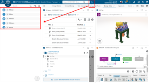
Every PCB need Mcad designer to make the product look awesome.It is the true fact that we have lot of companies which use traditional emails and other methods to communicate. Eradicating these methods of sharing information between electronics and mechanical designer in emails and other formats with the most advanced communication link between the two software tools which are in different places.
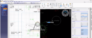
The designer can import the schematic design to the PCB layout in a single tool which vanish the data losses.
The components symbol in schematic sheet can be linked to component supplies which reduces the pressure of making the BOM in solidworks PCB which makes it different from others.
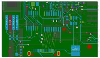
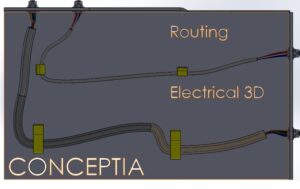
A smart routing technique makes the more complex design to simpler form with its differential pair routing technique.
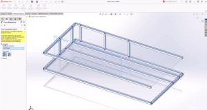
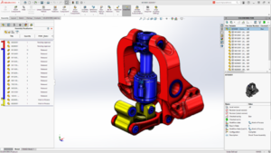
A 3D view of the PCB along with the layers can be viewed which helps in identifying the minute problems to give out the perfect output, which makes Solidworks PCB the perfect choice.
Solidworks PCB in Industries serve with its enormous features and user friendly icons. Implementing it in Industries is very easy and the designers can easily understand the features.
Unlike other software which use traditional method of sending email and other communication system to Mcad designer. Solidworks PCB with its most advanced technique of collaboration with M-cad tool helps in shaping the PCB with proper dimensions to fit into the mechanical enclosure and also reposition the components.
As design engineers spend most of the time in search of Components and its database. The schematic design in the tool has real time supplier link which reduce the burden of components search.
Layout design with auto routing and interactive routings helps the design to be faster which is very much necessary in this era to compete with other products.
A very special attribute of Solidworks PCB is its 3D visualization which helps in clearance checking as well as reducing the production of prototypes. All these features help the product to come out of industries as quickly as possible with less cost and no compromise in product quality.


I’m without a doubt satisfied to say it’s an thrilling publish to study. i examine new facts out of your article, you are doing a awesome mission.you could test our offerings
autocad training in indore
Leave a comment