

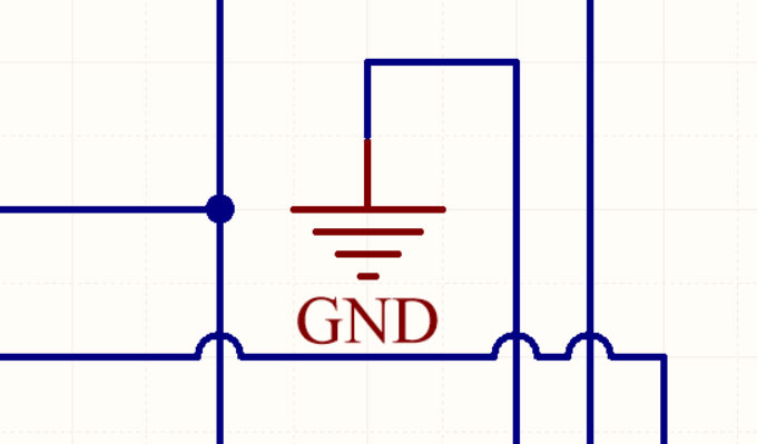
For any electronics schematic design cross overs/wire bumps are very important to connect one component to other component without interconnecting each other. In many conventional electrical schematic drawings, designers would manually draw the ‘wire bumps’ when they designing the schematic line would cross over other schematic lines, to identify the lines simply cross over each other are lines are connected to each other.
Cross over / wire bump in SOLIDWORKS PCB Design when creating Schematic
As electrical design packages have become more and more advanced, software packages can now be smart enough to determine on their own whether lines are connected are they are simply crossing over each other.
Similarly in SOLIDWORKS PCB we have the option to turn off or on these ‘cross overs’ as suits your own personal or company preferences and standards.
To turn on the cross over in the SOLIDWORKS PCB
File > system preferences > schematic > General tab under the general options we need to enable the Display cross-overs.
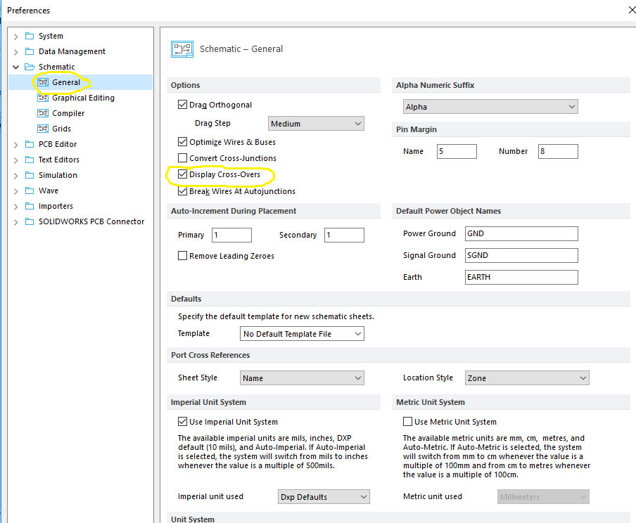
Once we have turned on display cross-over checkbox after Apply the changes now our ‘cross-overs’ have been automatically displayed on our schematic as we can see below image.


Any idea how to do this in Solidworks PCB 2018?
Leave a comment