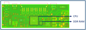
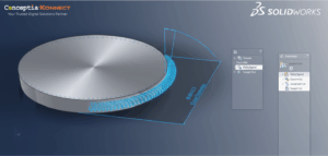
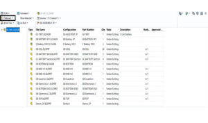
Printed circuit board is made by conductive tracks, interconnecting pads are via and other similar elements like etched from copper sheets and laminated onto a non-conductive substrate.
And we are inserting electronic device like Capacitors, resistors, integrated circuit and similarly other components are soldered onto the PCB whit the proper planned they are placing components in to the board. This components should be fit without interacting each other it’s should be placed within the smallest amount of space possible. This activates can be easily managed by using the SOLIDWORKS PCB.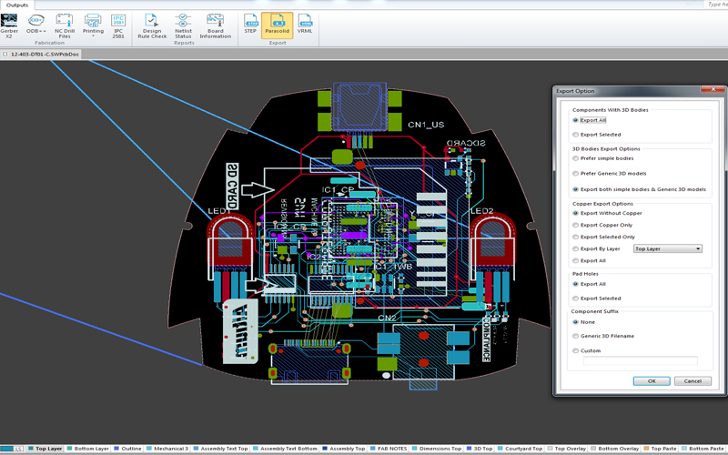
Exporting Copper Traces
SOLIDWORKS PCB Parasolid View
They are two ways to design PCB, Single layer and multilayer. This parasolid viewer its very help full in multilayer PCB. Because in multilayer PCB board, one or multiple conductor patterns inserted, layer by layer inside the board. In this we can easily captured each track passed out between sources to destination through the Export Copper Traces.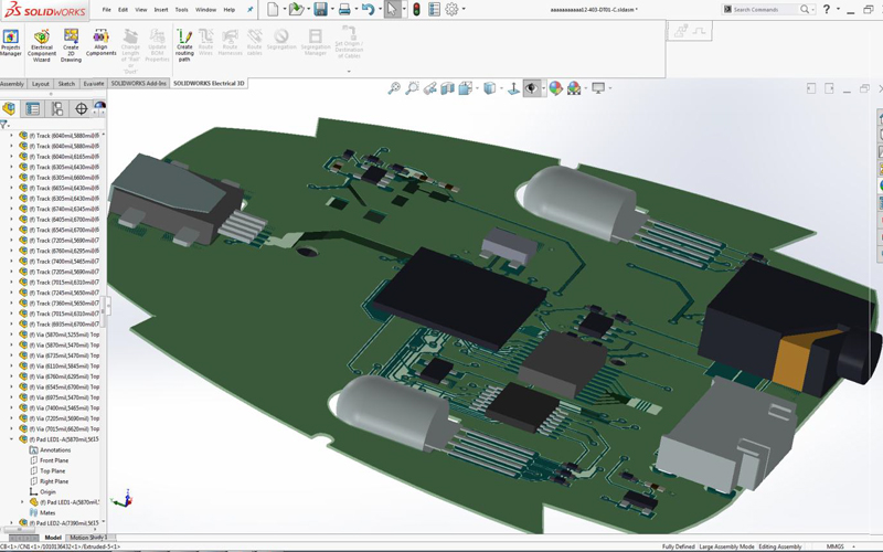
Multilayer internal view
By using SOLIDWORKS PCB we can able to visualize PCB body of surface tracks, included this we can able to visualize the internal layer tracks this is one of the advantages of using SOLIDWORKS PCB.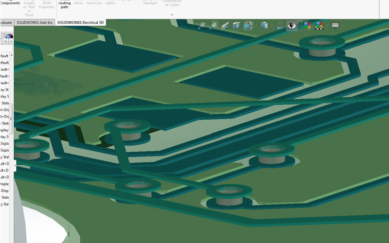
Multilayer internal view
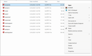
To export the 3D CAD file including all the copper traces, in the output creation tab go for export select the Parasolid, then in the pop up window we have a number of output creation option (here I am going for over all copper traces), go for copper export options and select the export all and save it into the required folder. After created the file if we open within the SOLIDWORKS we can easily visualized the entire copper traces by using a transparency.


